FDC6326L Overview
Description
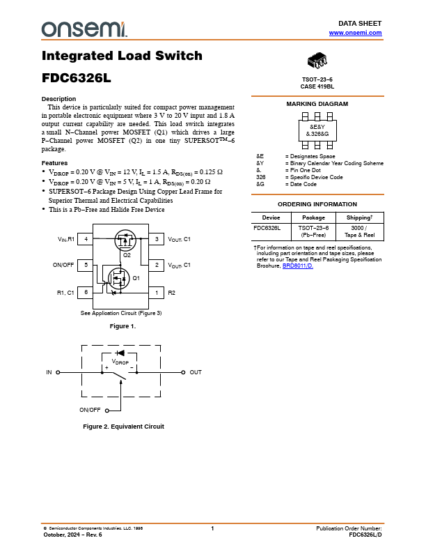
This device is particularly suited for compact power management in portable electronic equipment where 3 V to 20 V input and 1.8 A output current capability are needed. This load switch integrates a small N-Channel power MOSFET (Q1) which drives a large P-Channel power MOSFET (Q2) in one tiny SUPERSOTTM-6 package.
Key Features
- VDROP = 0.20 V @ VIN = 12 V, IL = 1.5 A, RDS(on) = 0.125 W
- VDROP = 0.20 V @ VIN = 5 V, IL = 1 A, RDS(on) = 0.20 W
- SUPERSOT-6 Package Design Using Copper Lead Frame for Superior Thermal and Electrical Capabilities
- This is a Pb-Free and Halide Free Device VIN,R1 4 ON/OFF 5 R1, C1 6 Q2 Q1 3 VOUT, C1 2 VOUT, C1 1 R2 See Application Circuit (Figure